
There's a persistent myth in the electronics commnity that if you want programmable logic to interface with 5V these days you have two options – very old CPLDs (Complex Programmable Logic Devices) or use level shifters to convert the 5V down to 3.3V as there are no 5V FPGA anymore. Well, I'd like to spend a few minutes busting this myth.
Level Shifters
A quick aside, if you need level shifters or feel safer with them, then that's fine, I'm not at all condemning their use. And I would like to give a huge shout out to the A314 project that proved that the CBT(D) devices are absolutely fine for anything 5V TTL. This is because 5V TTL is designed to respond to a high logic level as low as 2.0V which also fits nicely within the range for 3.3V CMOS devices.
True 5V FPGA
So lets get this out of the way right now – there is a true 5V FPGA on the market and it's a pretty great chip. The AT40K series has been in production now since 1997 and as with their PIC microcontrollers, Microchip seems hell bent on never deprecating these parts. The largest of these is the AT40K40 with up to 384 IO pins, 18Kbit of internal RAM and 2,304 logic cells, but even the smallest, the AT40K10 with only 576 cells has VASTLY more logic room than even the largest CPLD.
It's interestingly difficult to just "browse" to these from Microchips website though, so I've included links.
| Part | Logic Cells |
RAM (Kbit) |
AVR |
|---|---|---|---|
| AT40K10(LV)/(AL) | 576 | 4.5 | No |
| AT40K20(LV)/(AL) | 1024 | 8 | No |
| AT40K40(LV)/(AL) | 2304 | 18 | No |
| AT94K05AL | 576 | 4.5 | 25MHz |
| AT94K10AL | 1024 | 8 | 25MHz |
| AT94K40AL | 2304 | 18 | 25MHz |
| AT94S05AL | 576 | 4.5 | 40MHz |
| AT94S10AL | 1024 | 8 | 40MHz |
| AT94S40AL | 2304 | 18 | 40MHz |
They even have features few other FPGA have:
- partial reconfigurability (they call caching)
- highly configurable IO with delay/slew
- the 's' variants include configuration ROM on-chip
Its logic cells are not directly comparable to other FPGA chips (whose are?) with two 3-input LUTs that can be chained into one 4-input LUT, includes the very common DFF with tri-state output and internal feedback, internal 2-to-1 mux and hard AND gate for efficient multipliers.
But a modern FPGA it is not. Propagation delays in-fabric are pretty high compared to modern logic. It's large enough and fast enough though to be a great bus-bridge or maybe even a simple microprocessor. As with any FPGA these days, it supports VHDL and Verilog, so it's just a matter of remapping the pins.
So there … there's a real, bona-fide 5V FPGA that's still in production.
Note: The LV and AL are not marketted as "true" 5V, they are 3.3V devices but remain 5V "tolerant." What this means is that the output of the IO is 0~3.3V but the input can safely tolerate 5.0V levels. So quite literally, it's "tolerant" of 5V parts, but is not, itself, 5V anymore. That's fine, because 5V TTL does not need "true" 5V outputs.
However, in the datasheets, the absolute maximum for the voltage is still listed at 7.0V which means in actuality, these are still 5V parts. Even the FPSLIC (with AVR microntroller) list 5.5V as the maximum for input voltage, so yes, even it is a 5V part – with the caveat that the AVR operates faster with lower voltages – you probably won't get 25MHz above 3.3V.
A Modern Alternative
The iCE40 is the successor to the iCE65 P series from SiliconBlue which was marketted as 5V tolerant. There is no clear evidence that the iCE40 was ever intended to also be 5V tolerant, however, in 2021 it was discovered quite by accident that the iCE40 HX might be. When interfacing with a PS2 keyboard, it was discovered that the iCE40 did not, in fact, release the magic smoke when absent of any external current limiting resistors.
With a 47K series resistors the following was observed.
| Source Voltage |
Pin Voltage |
Leakage Current |
|---|---|---|
| 5.0V | 5.00V | 0 |
| 6.0V | 6.03V | 550nA |
| 6.5V | 6.35V | 3uA |
| 8.0V | 6.39V | 34uA |
| 10V | 6.40V | 77uA |
| 20V | 6.41V | 290uA |
It should be noted that 20V is already in the realm of "distructive testing" for any 3.3V part.
Document Archaeology
There is no record of any iCE40 datasheet prior to 1.31, even on the Wayback Machine and there is no mention of 5V tolerance there or on any of SiliconBlue's saved webpages from the era. There are some interesting things to note though; there are signs this information was scrubbed and 1.31 shows this – in progress – as it contains mention of JTAG which was removed in all later literature from Lattice and has a weirdly-round 4.00V as the absolute maximum they later nerf further to the more "common" 3.60V found with 3.3V logic.
Hmmm…
The IO structure is identical as all the drawings are directly ripped from earlier SiliconBlue drawings and it's probable they used the same macro cells. It's worth adding that TSMC's 40nm process likely has the same 5-7nm thick oxide layer, so 5V tolerance is likely.
Why Would They?
I mean, this is pure speculation and there's a lot of conspiracy theories out there as other manufacturers have pulled 5V tolerance for a number of reasons from not wanting to look antiquated, confusion over "real" 5V parts and 5V "tolerance" as well as the additional burden of testing.
However, I think the reason is actually simpler and more obvious – temperature range.
The iCE40 is marketted as a mobile FPGA and supports an impressive 125°C junction temperature tolerance. It can get pretty roasty inside of those smartphones and tables with little-to-no ventilation, and 5V would absolutely bring that maximum down.
For retro use, that doesn't matter.
The Pudding
1. Faith
A while back, Kipper2K and I worked on the Amiga Replacement Project and came up with a versatile DIP-sized board that could replace any 40 or 48-pin DIP chip with little modification. He put together a couple of Faith board (Denise replacements) before disappearing.
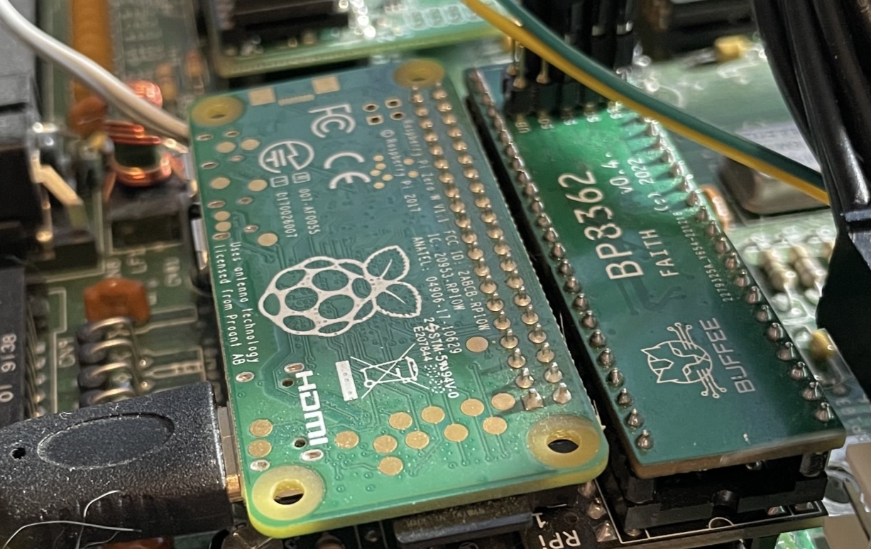
In the interest of testing, the first step was actually implementing Denise into FPGA. On January 3, 2026, I got the first good output from my CDTV. Well tickle me gingers.
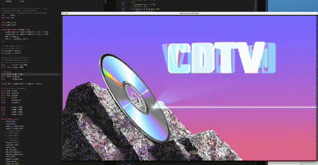
I was worried that maybe it would be darker or something, but nah, this looks fantastic. It's not the best code and it was horribly broken when trying some demos, but it proved the case. I've put all the code over in the Amiga Replacement Project repository, but at the moment, it's not 100% Super Denise compatible and there's a bug in the board that has disabled the on-board Flash.
Side note: I'm really impressed with yosys/icestorm.
It's been running on and off now for over a month with no degradation, but this isn't proof that it'll last, that's going to take more work.
2. Destructive Testing
I recently managed to get a bunch of equipment to start making some boards myself. One of these was a hot plate and that got me thinking – I could put my 500+ upside down on there and cook it at 80°C for a few days straight and then redo the original current test. If the pin was degraded in anyway, we should see more leakage; i.e., more current being drawn or a lower voltage limit.
I'll need to set up a little Linux server to do this though, since, because of the bug, the moment I unplug my MacBook, Faith will reset and then clear it's config.
This should prove whether the part is really 5V tolerant or not. I personally believe it will be a huge boon to the retro community at large if this works; this reduces parts, board complexity and size, making these little DIP and PLCC inside boards possible.
I'll post here when this is done.