
Well, have to admit, I had missed a lot of minor design issues, but now that we've gone through the complete checklist and have finished our first professional review cycle, I can confidently say we're very near getting our first boards made. I even managed to shrink the board a little bit so that it fits precisely into a 64 DIP socket with zero overhang! A quick run down of all the major bits:
-
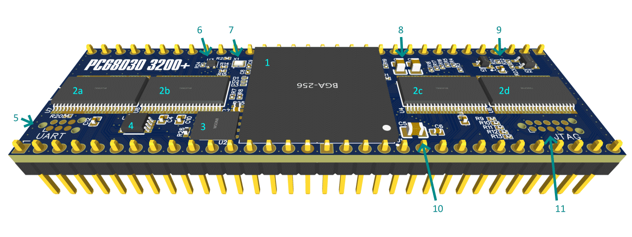
The big BGA 256 in the middle is the main CPU, an OSD335x-SM. This comes pre-equipped with either 512MB or 1GB of DDR3L-800 SDRAM as well as all power management and related passive components.
-
The four chips surrounding the CPU are our level shifters; four 20-bit SN74CBTD16210 chips. Since these can do 20-bits, it will be possible in a later revision to omit one of the chips, saving some precious board space. There are also some smaller package options to consider as well.
-
The first small chip on the bottom is the SPI Flash; 16MB of it, specifically. This may shrink before mass production, but right now it's a very generous size just in case.
-
This is new; it's to isolate the UART from the CPU incase you power-off one unit without powering off the other.
-
Also new is the TC2030 (Tag-Connect) form-factor UART connection. TX is on pin 2 and RX is on pin 4; the other pads are all ground. This saves a lot of room over the older 0.1" header and with a ground, should be more robust. The UART also serves as a back-up programming port as the Flash can be programmed using XMODEM.
-
A small addition to perform the warm-reset. Crazy as it sounds, the OSD335x has a 1.8V power good OUTPUT and a 3.3V warm reset INPUT.
-
This is the 24MHz crystal. I seriously contemplated the idea of making this a programmable osciallator but between running out of room and the complications with the internal clock circuitry this would create, I veotoed myself.
-
This is 55uF of bulk capacitance on the 3.3V line as specified in the checklist
-
This is the clamp circuit required to avoid destroying the chip during power-down. It may not be required since we're not heavily using either the 1.8V or 3.3V power rails. Most of our logic runs at 5V. Anyway, this stops the difference from the 1.8V rail and 3.3V rail from exceeding 2.0V which apparently is "bad".
-
This is a high and low frequency capacitor on the 5V line to help filter out the (possibly) noisy power from the Amiga. The bulk capacitance also helps a little on power dips.
-
Finally the JTAG is implemented as a TC2050 connector to the core. JTAG or UART may be used for programming, but JTAG is the only way to debug code efficiently, especially during the initial firmware development phase.
This is all built on eight layers of PCB; and don't worry, we have a ground plane! Three of them in fact, for some nice, stable signals.
Well, hope this gives you an idea of what's going into the Buffee Accelerator! At least in terms of hardware.